HV Power Supply: Custom H-Bridge

I will first be creating a custom high-voltage H-Bridge PCB that will invert my HV DC bus (rated up to 600V @ ~3A) to a bipolar square wave.
Component Choice
The first step when building a PCB is creating the functional schematic, however without the exact components, the exact pin connections, number of inputs/outputs, and other component specifications, the schematic can't be made.
Choosing the components for the task, especially for an SMD board such as my own, requires choosing a manufacturing and assembly service. I chose JLCPCB because of their good reputation and large assembly parts catalog. On their website I searched for parts using their library and filters, ensuring each part I chose had over 1000 in stock and was "active" and not "obsolete".
Thus, my first step in the design process is to create a block diagram for the exact genres of components I expect to need (organized by function), and then finding specific components from the JLCPCB catalog that fit my specification requirements, and then reading each datasheet for the "typical application" schematic for my use-case to find what supplemental components I will need.
An H-Bridge has a simple function and can be broken into 2 functional blocks: The switching components (i.e. MOSFETs) and the gate drivers, that need to be compatible with each other.
- In my case, because I may want to scale up this PCB in later high-power iterations (since right now I just want to make a proof-of-concept design), I chose the IPD80R360P7 13A 800V N-Channel MOSFET because of its high ratings and relatively low on-resistance of 360mOhm.
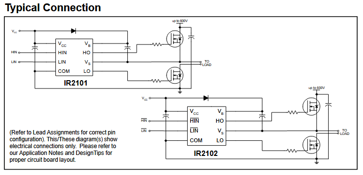
- I chose the IR2101 gate driver since it can bootstrap up to a floating 600V node which should be more than I need. The gate driver typical application is below: (obtained from this datasheet PDF)
- This thus requires a HV bootstrap blocking diode for 600V to VCC (thus blocking up to 588V in my case using 12V VCC), where I chose the US1MF 1000V 1A 75ns reverse recovery time diode.
- The capacitor from 600V to GND for each half-bridge needs to have a voltage rating >600V and value ~0.1uF to reduce the voltage spikes caused by high currents and inductance in the traces during high-frequency switching. I chose to use one X7R 1kV 0.1uF +-10% capacitor for each leg of the H-bridge, part C1812X104K102T.
- Each gate driver also requires a local decoupling capacitor, I just used a simple X7R 100V 0.1uF +-10% capacitor for each gate driver, part CL21B104KCFNNNE.
- From the node at the gate driver output to the MOSFET gate, gate capacitance and trace+lead inductance can create a series resonant tank that causes ringing and irregular switching of the MOSFET. A resistor is often used to prevent this by damping the LC tank. I used a 4.7ohm 1206 gate resistor part 1206W4F470KT5E for this task.
- In addition to the gate resistor, a small-signal gate diode in parallel with the resistor and reverse-biased relative to the gate driver output allows for the gate capacitance to discharge quickly and thus decrease the turn-off time. I used the 1N4148W 100V 150mA 4ns reverse recovery time SOD-123 diode for this task. This is optional but I chose it to ensure the H-Bridge module works as intended.
- I am going to use a 5-pin screw terminal connector 1725685 for the 4 MOSFET gate input signals and their ground reference, a 3-pin 650V screw terminal connector 1717732 for the input +VDC power, +12V power, & power GND, and a 2-pin 650V screw terminal connector 1717729 for the output bipolar square wave.
- I also will use 4 M3 mounting holes on each corner of the PCB to eventually mount it to an enclosure and connect it to subsequent power supply modules.
PCB Layout:
The main things I considered when placing my components were the recommended layout by datasheets and application notes for what I intend to do, and general PCB layout rules and standards. My main resource for layout in general was this TI application note. For the gate drivers, my main resource was this application note.
Notable extra considerations
High Voltage Clearance:
Because my PCB will use voltages above 50V, clearance considerations are especially important. I am going to assume 600V-level clearance required for all nodes at +VDC relative to all nodes at GND, 12V, or logic-level input, since that is the limit my bottlenecking PCB component (the gate driver) can handle. For clearance considerations I will use the IPC-2221A(L) standard table for electrical conductor spacing, given below:
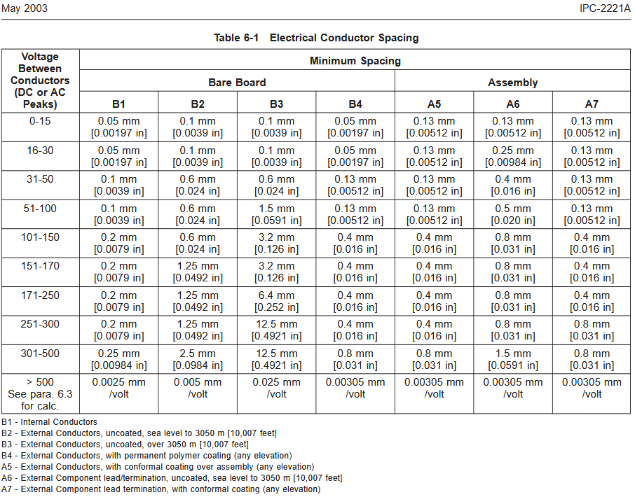
This can be summarized for my application with the following 3 rules:
- Exposed metal (TH component leads and SMD pads/leads) distance to exposed metal must be >3mm.
- Surface-level copper traces covered by solder mask at 600V must be >1.83mm from low voltage surface-level copper traces covered by solder mask.
- Internal copper traces at 600V must be >1.5mm from low voltage internal copper traces.
Stitching Vias:
Due to the orientation of the components and routing limitations, in order to keep the high-noise parts of the circuit (diodes, switching nodes, high-current traces) physically separated from the high-sensitivity parts of the circuit (input signals, output signals), I will be using a 4-layer PCB with the signal+power, GND, power, GND stackup. This, along with 1oz internal copper weight (as opposed to the default 0.5oz) will give strong GND return paths for all traces, adequate space for wide power traces, and physical separation between internal power routing and sensitive signal routing on the surface of the board.
This necessitates stitching of the GND planes together so their potential stays consistently at the same value throughout the plane. This will be done by placing vias generously across the board (ensuring 1.5mm clearance from any HV nodes) between the ground planes.
Mounting Hole Vias
The M3 mounting holes will have vias in a circular pattern on their pad surface. This strategy, as explained in this Stack Exchange thread, is to ensure mechanical robustness and strong electrical connection when mounting the PCB to an enclosure using a screw or bolt. The vias will do this by raising the surface of the PCB a tiny amount, allowing the screw to contact the vias and ensure consistent contact with the desired node.
Thermal Vias
In this PCB, the power-dissipating components can generally be assumed to be solely the MOSFETs, since their conduction losses due to RDS(on) at high currents will dissipate power according to \( P_{cond}=I^2R \), their switching losses will dissipate power according to \( P_{sw} = V_{in} \times I_{out} \times f_{sw} \times \frac{Q_{GS2}+Q_{GD}}{I_G} \), and gate losses dissipate power according to \( P_{gate}=Q_{G(total)} \times V_G \times f_{sw} \). Source.
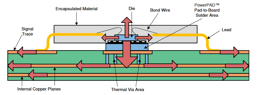
Due to this, heat will be produced and conducted away from the MOSFET semiconductor through the encapsulated material, through bond wires and leads, and through the metal pad connections. The greatest amount of heat is transferred out through the pad connection because of its direct metal-to-metal contact. This allows for the device to generate and dissipate a large amount of heat unless bottlenecked by high thermal resistance (i.e. thin copper traces leading outwards from the MOSFET). To avoid this bottlenecking, thermal vias allow direct metal-to-metal connections to large copper planes/zones within the board that have high surface area, acting like a heatsink within the board. This is illustrated in the image below, obtained from the TI application note.
Component Placement:
First, I placed the IPD80R360P7SAUMA1 MOSFETs in the half-bridge configuration recommended in the application note for that MOSFET package: (apologies for the bad quality, that is what the application note provides)
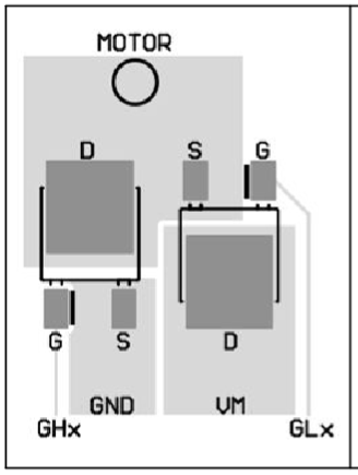
I then placed the 2 legs side by side with the 2-pin screw terminal for the output voltage on top between them. I separated the 2 legs a little in order to make space for the gate resistor and diode between them from the low side of the left leg.
Next, I placed the gate drive resistors and diodes as close to the gate pins of the MOSFETs as possible.
Next, I placed the 2 decoupling capacitors between VDC and GND on the H-bridges as close as possible to the MOSFETs to aid in noise reduction and local inrush current demand.
Next, I placed the gate driver ICs below each half-bridge with their respective boostrap diode & bootstrap capacitor as well as their respective decoupling capacitor. I did this as close as possible to the MOSFETs to reduce the trace length of the gate signals, but making
Next, I placed the 3-pin power screw terminal on the bottom of the PCB and the input signal 5-pin screw terminal also on the bottom of the PCB.
The 4 M3 mounting holes were placed on the corners of the PCB, and stitching vias between ground planes were added to the spots with no traces nearby.
PCB Manufacturing
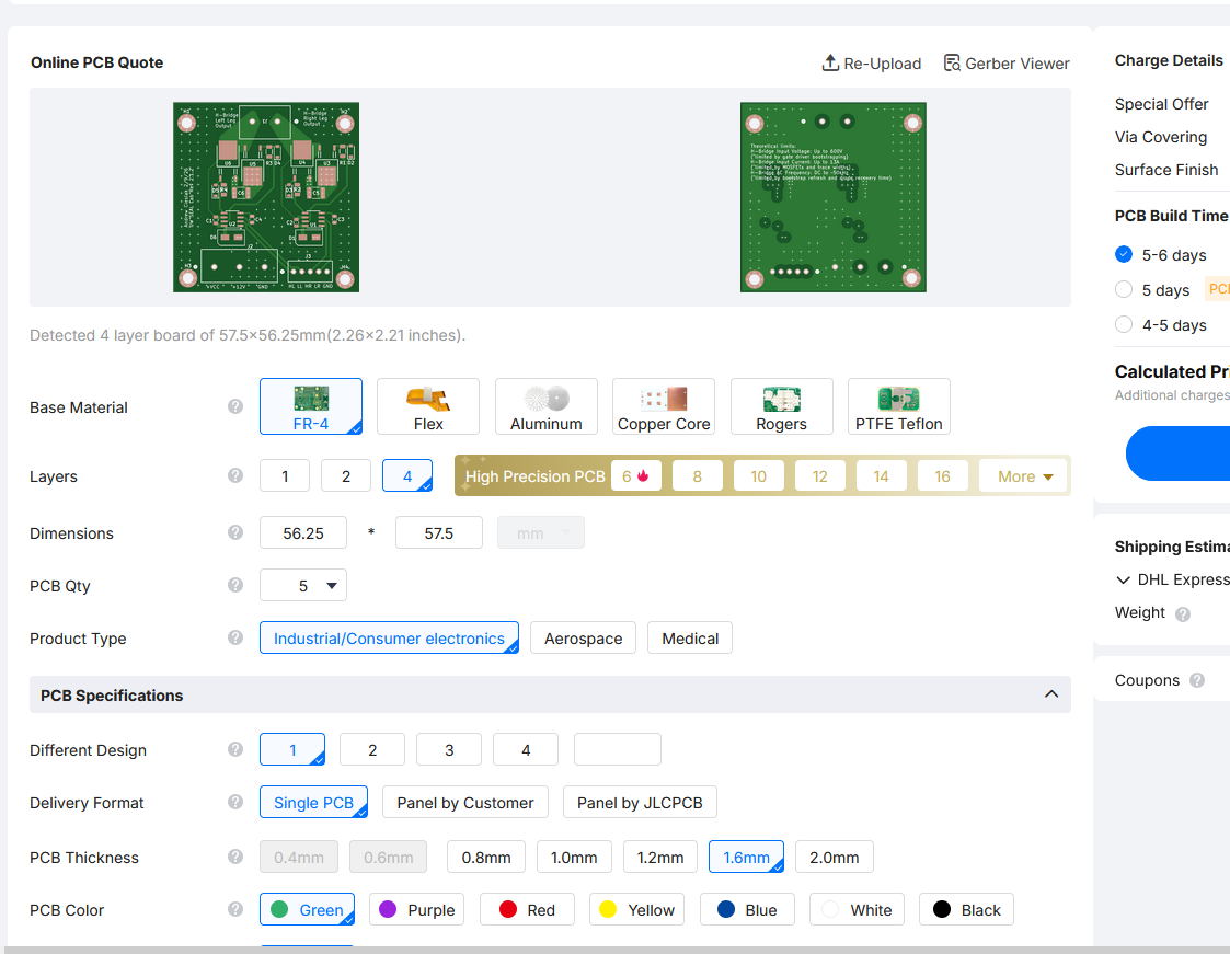
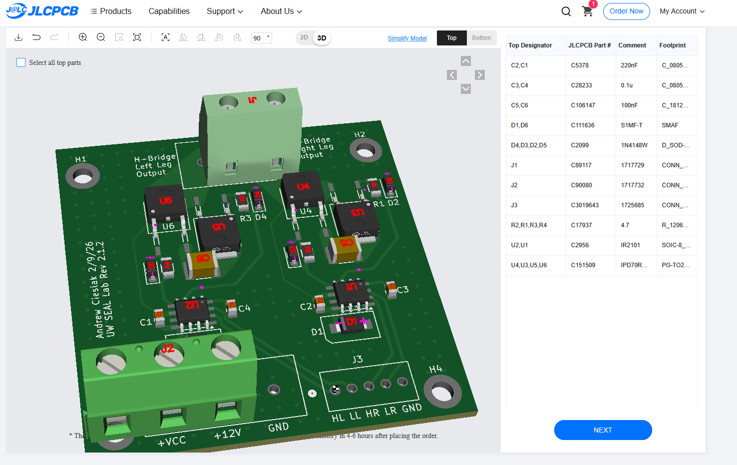
After I made sure first that all of my components were available from JLCPCB, I exported the GRBR and DRILL zip file to JLCPCB with the drill file origin at the bottom left of the PCB.
Next, I selected the appropriate options for my PCB, such as 1oz internal copper, 4 layer, green color, etc. Then I made sure to select PCBA and clicked "next" to set up the PCBA process.
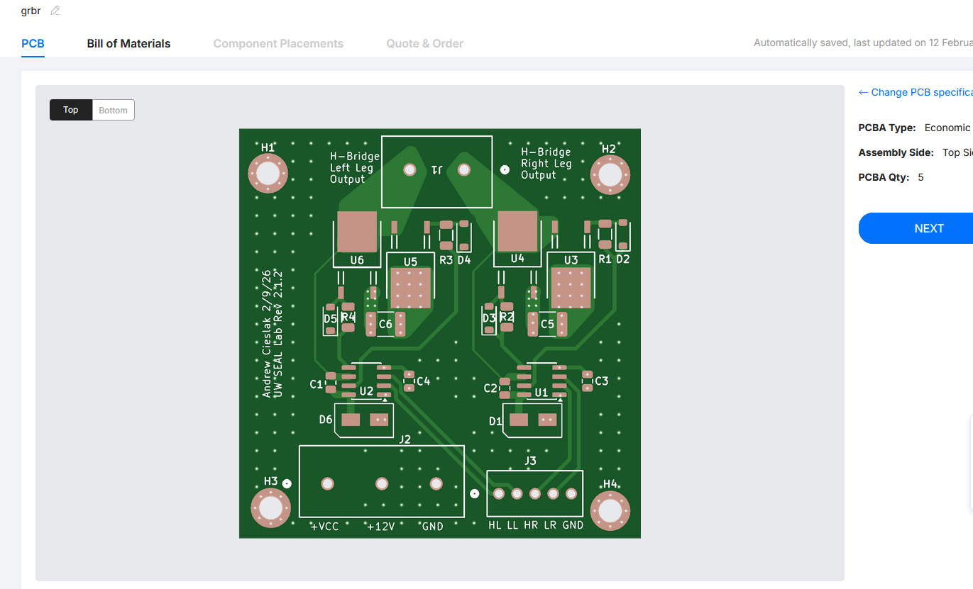
In the next menu, it shows a preview of my PCB, so I just pressed "next".
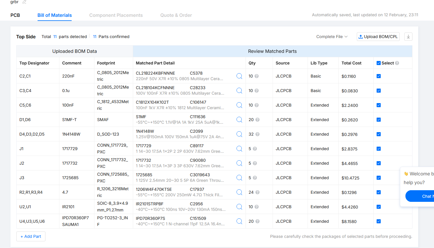
In this menu, I get an overview of the parts I will be using. I pressed "next" since I already made sure these were available.
Now here, I had to manually rotate and re-align components to be where I expected them to be, specifically the screw terminal connectors and gate drivers.
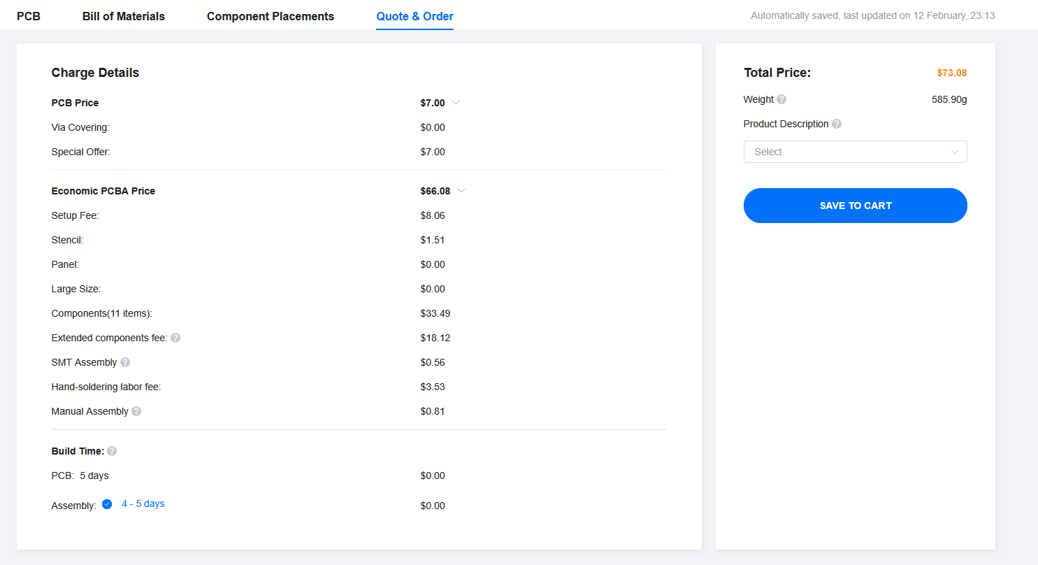
Now I just save the PCB to cart, and order, and I'm done! Next will be testing of the H-Bridge once it arrives.
3/2/26
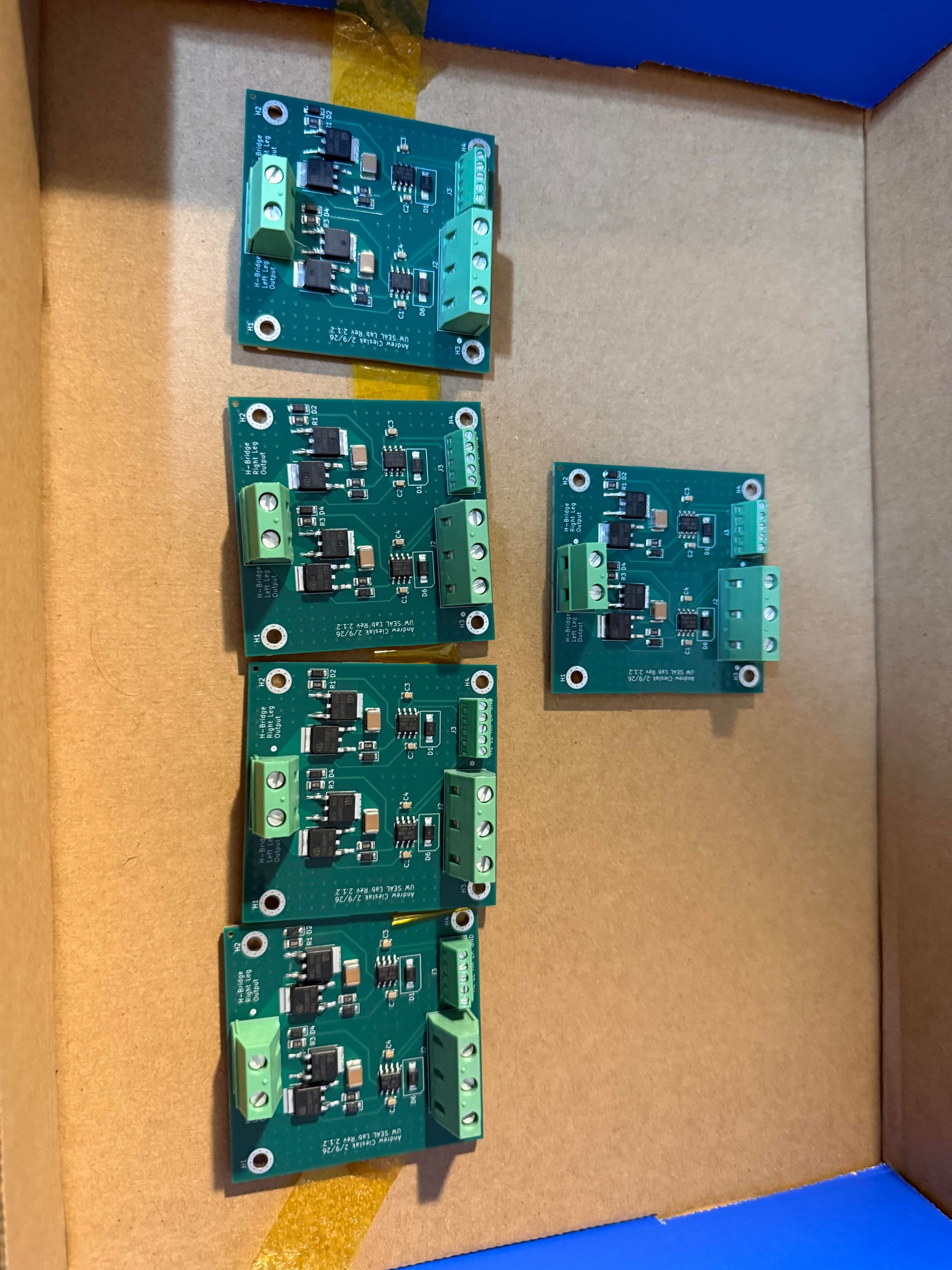
My H-Bridge arrived!!! It ended up actually being $200 for the 5 assembled PCBs which is quite a hassle, but because this project is mainly for SEAL at UW which I am a part of, I got reimbursed by them for it. I really hope it works so we can have functional HV power supplies to play around with!!
What happens now for this stage is testing, which I can do via a few simple steps:
- Create the 4 gate drive signals with my Analog Discovery 1 that I got for free from my community college assistant professor in Physics. I can do this by using the Waveforms application on Windows or my Macbook, and ensuring the signals are synchronized (first checking with my Hitachi V-665A oscilloscope that I also got for free from a Facebook Marketplace electronics lot).
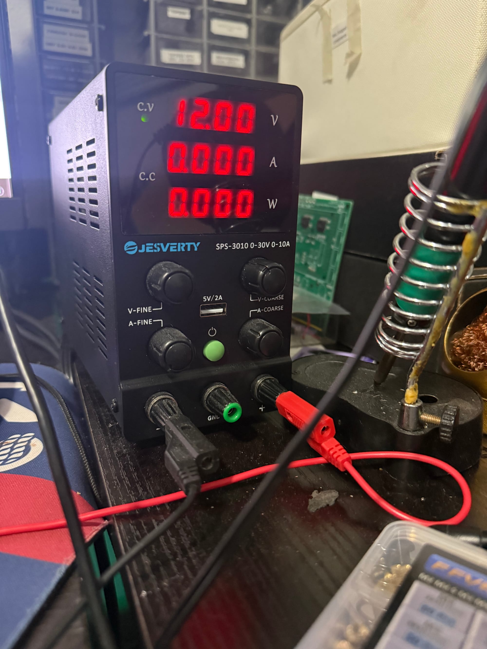
- Supply 12V to the 12V supply terminal pin. I can do this via the Analog Discovery 1 OR from the SPS-3010 CC-CV 0-30V power supply I borrowed from the lab since it didn't work as well as they wanted, and they got a new one.
- Supply the "HVDC" voltage to the HV pin. This can withstand (hypothetically) up to 200V, but for this test to simplify things, I will begin with the same 12V that I am powering the gate drivers with (coming from the SPS-3010 supply).
Testing!
For my testing, I just want to confirm that:
- The Analog Discovery produces signals as expected
- My Waveforms configuration produces 2 pulse signals of equal on-time (to eventually avoid flux walking, i.e. accumulation of DC bias in the transformer that eats up the flux and saturates the core), a dead-time between them (guaranteed OFF to avoid both square waves being on at the same time, i.e. shoot through), and from 0V to 5V.
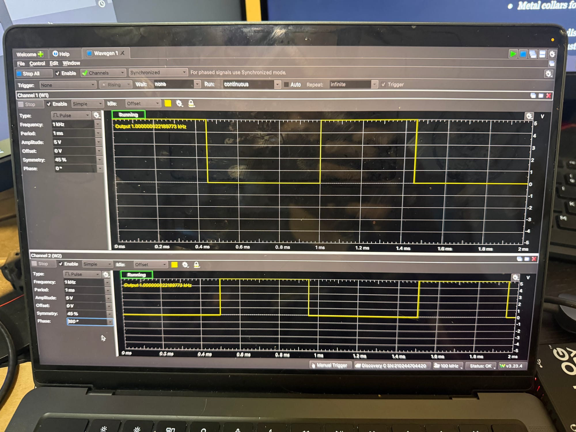
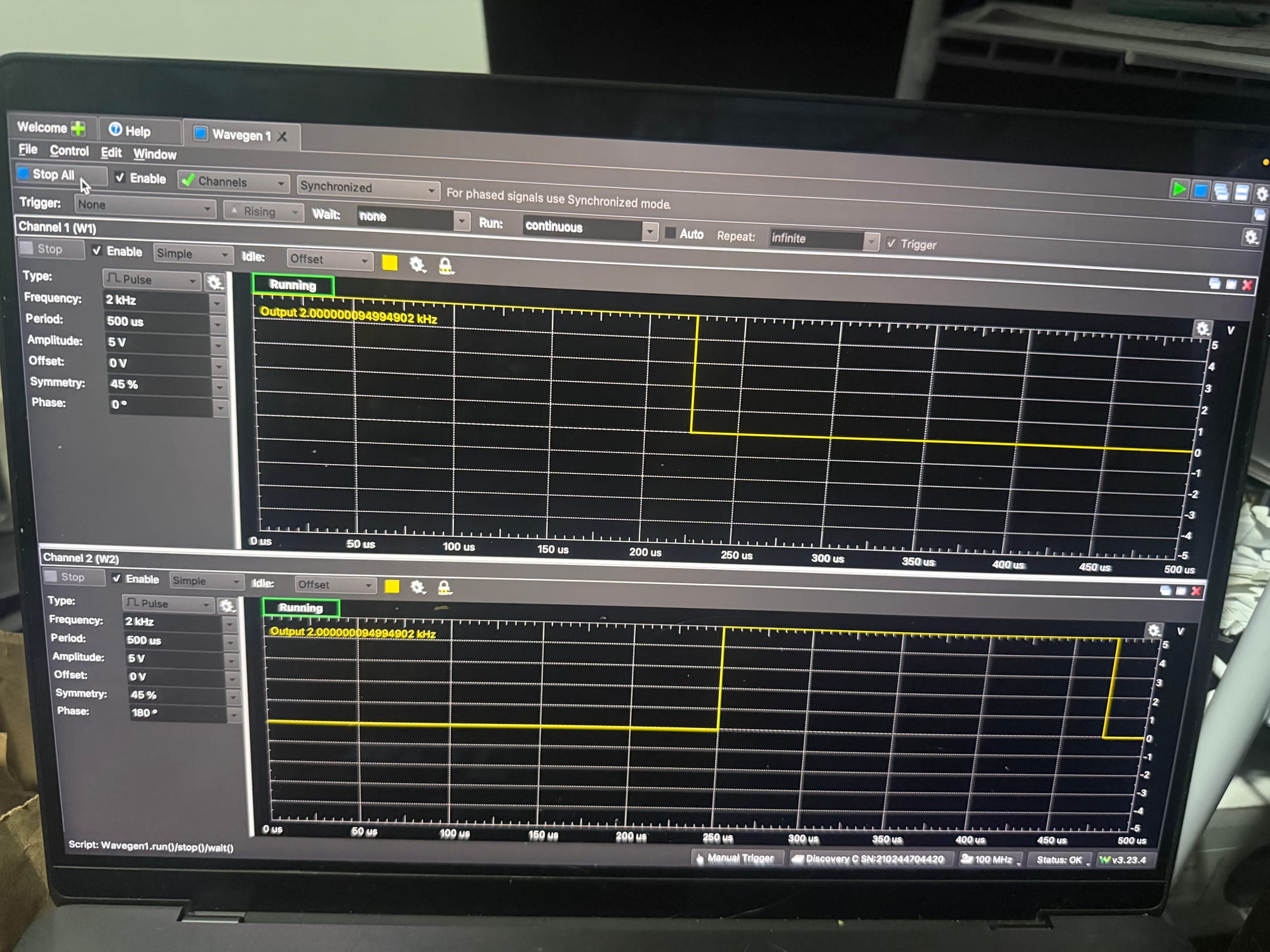
To do this, I first set up the Waveforms configuration on my Macbook, which consisted of 2 synchronized "Pulse" signals from 0V to 5V with 45% duty each, both at 1kHz with one being 180 degrees out of phase of the other. This is shown below:
For the first test, I just turned on my Oscilloscope, connected one probe to each of the W1 and W2 signal outputs and the probe grounds to the GND of the Analog Discovery 1, and got the below signal once scaling correctly:
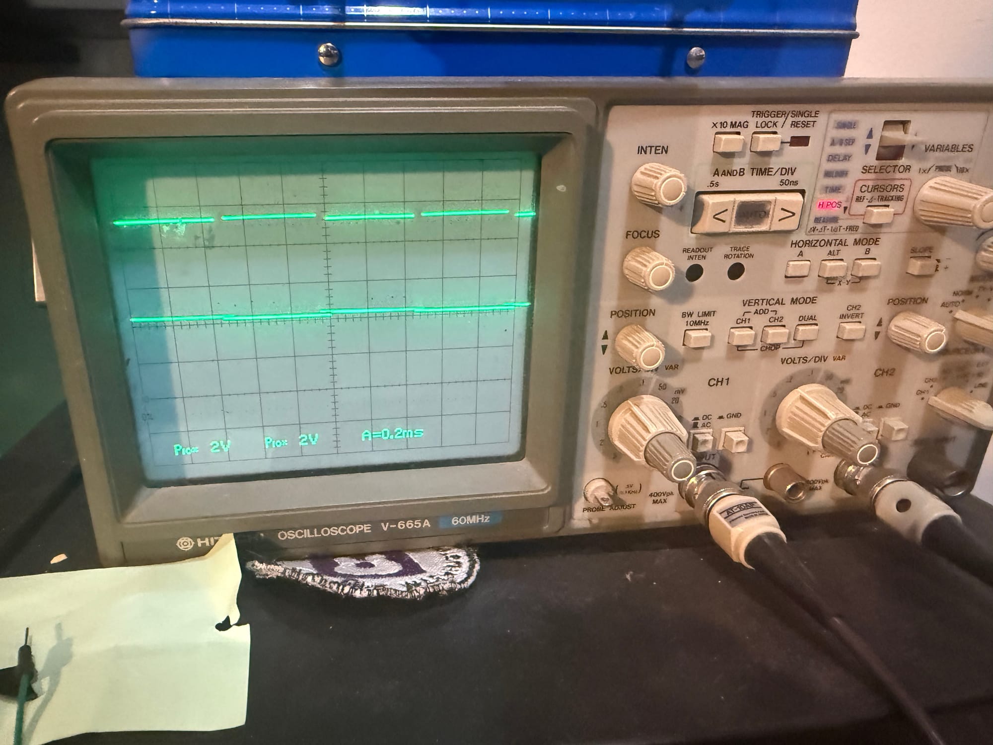
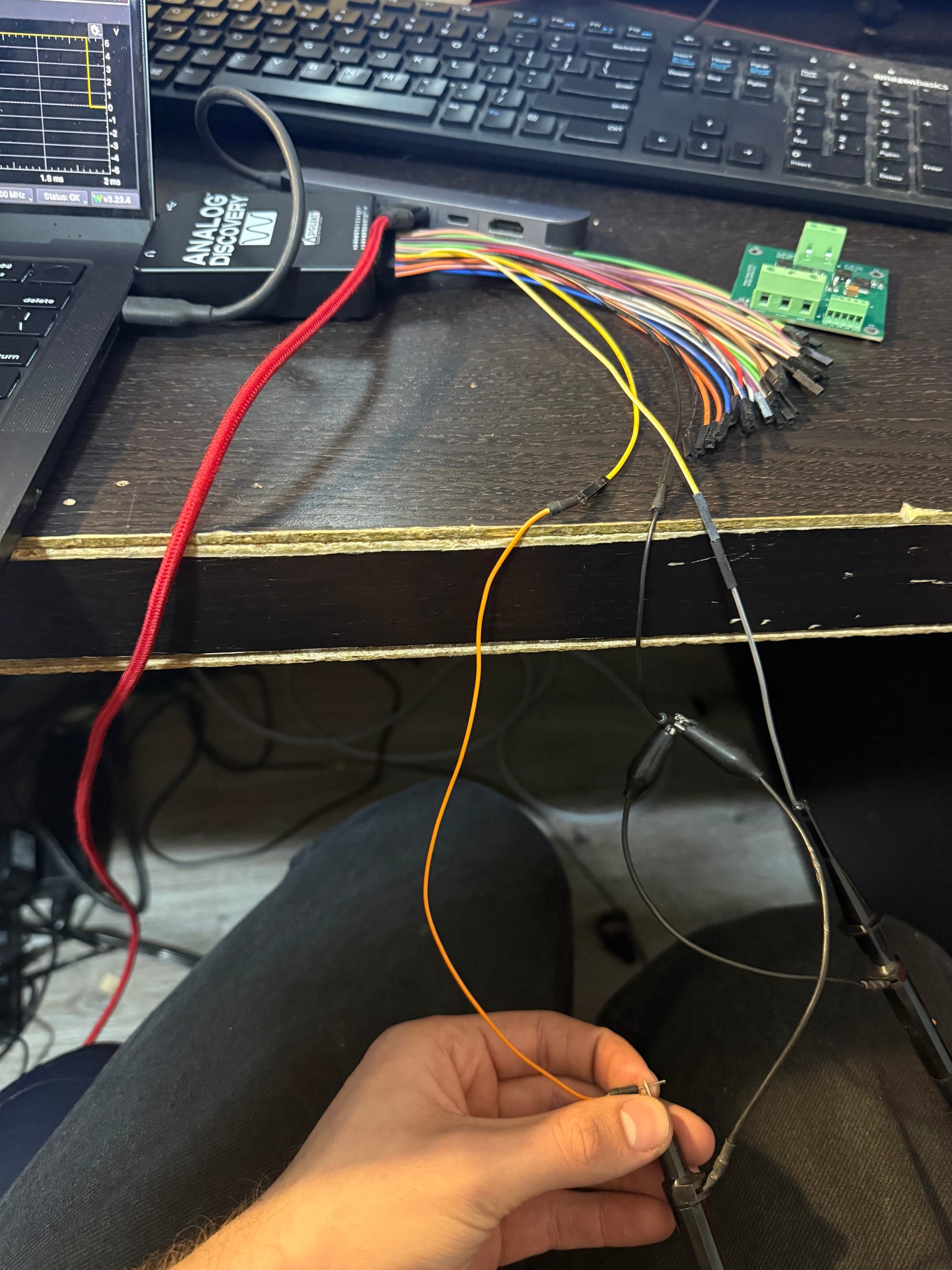
Perfect! There is visible dead-time, and the signal amplitudes are as expected. It's hard to confirm the on-times are exactly the same, but they visually look the same, so I will assume so for now. Here was my setup on the Analog Discovery side:
Now that signal testing worked, it's time to actually apply power to the H-Bridge PCB! First though, I'll just apply 12V to the 12V pin and the DC supply pin, and see what happens with my Oscilloscope.
Note: I just realized that when the inputs aren't being driven, they float, and that can cause issues with what the gate driver sees (duh). I should have put pull-down resistors on the HL, LL, HR, LR inputs (since both HIN and LIN in the IR2101 datasheet are output HIGH when input is HIGH). Luckily, I can just implement pull-down resistors on the board(s) that drive the inputs, but in my next iteration I will definitely include those. When testing, I will utilize pull-down resistors between the Analog Discovery and the PCB by using a breadboard in between as an intermediary. I'm going to use 2 1kohm pull-down resistors.
Since there are 4 signal inputs (I made it this way to allow for phase-shift modulation which requires independent driving of each MOSFET) I will be driving diagonal inputs with the same signal (Meaning HL+LR will be driven identically, along with HR+LL opposite to HL+LR). Because of the above note, I will also be using 2 1kohm resistors to ground at the signal pins, one for each pair. This circuit configuration can be seen below:
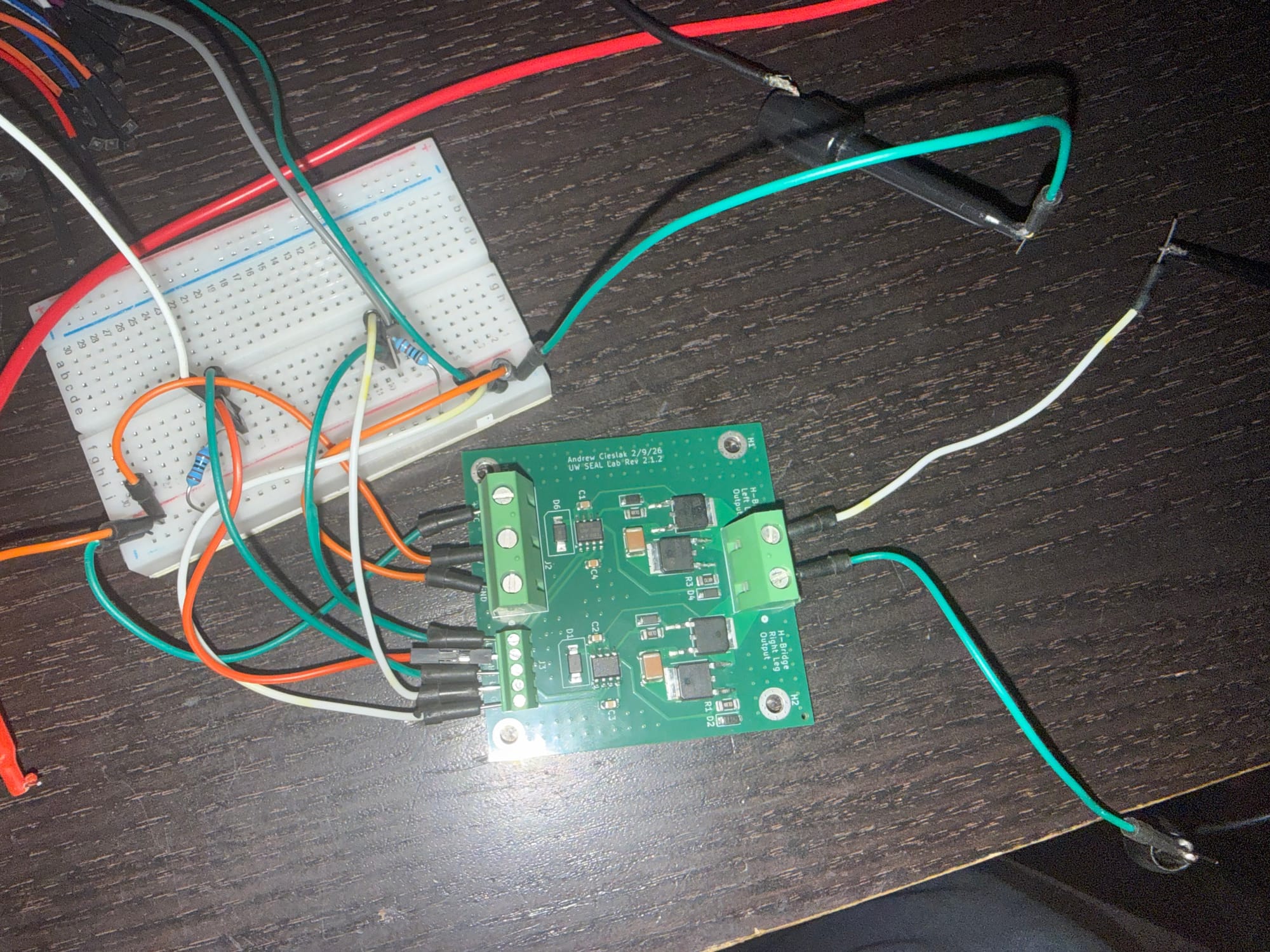
On the right is the output with my oscilloscope probe attached across H+ and H-. Power is +12V, connected to both the gate drive power and H-Bridge supply input. In future high-voltage iterations, the +12V and High-Voltage nodes will be independent.
As explained above, LR+HL and LL+HR are connected and brought to ground each with a 1kohm resistor, and then those two are driven by the Analog Discovery 1. The Waveforms signal config. is shown again below:
The resulting output from this is below!!:
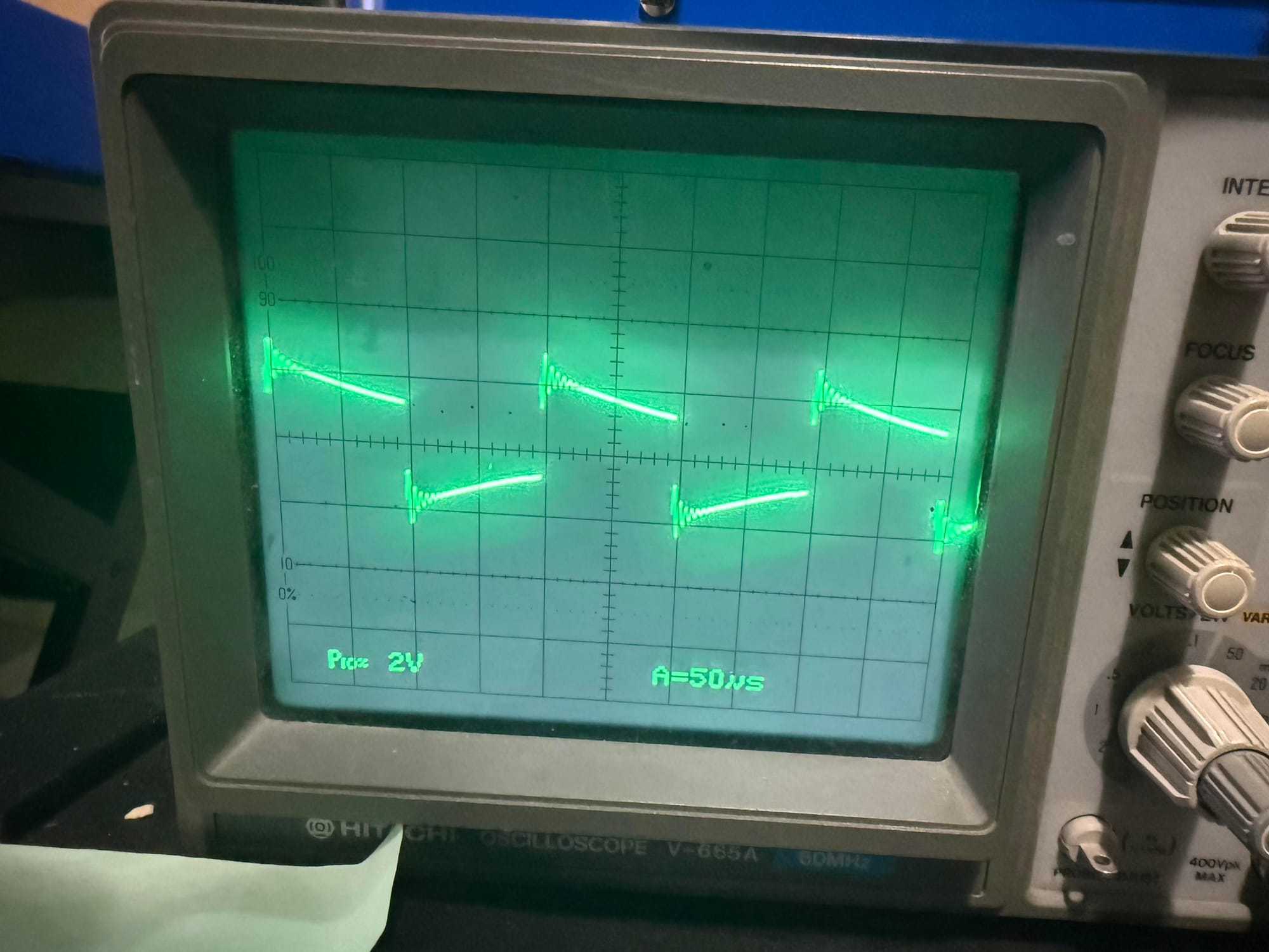
Uhhh...what happened? Why is the voltage decreasing? It almost looks like a capacitor-esque decay??? And why is the voltage so low?? I would expect it to be 12V in amplitude, or at least 5V since the logic input is 5V? Did I make my PCB wrong?!?!? I could have wasted $200 the lab gave me!! How will I explain this to my lab director!!!!???
Oh wait...when checking continuity between the output MOSFET node and the output screw terminals with a multimeter, there seems to be a break...I replaced the jumper wires and re-screwed the terminals, and now the continuity works! Now let's see how the output looks...
YIPPEE!!! THIS PART OF MY PROJECT IS COMPLETE!!!
Improvements:
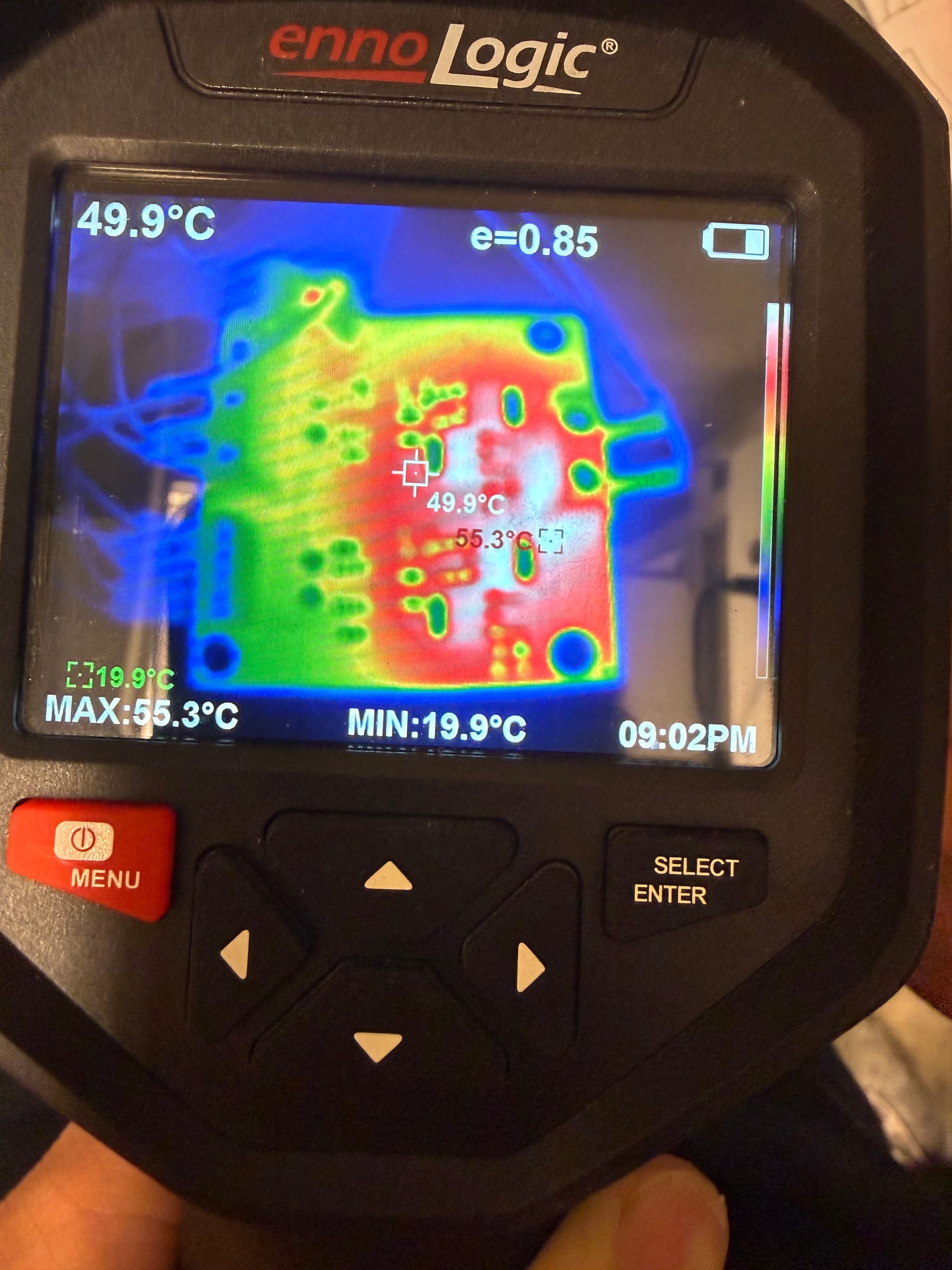
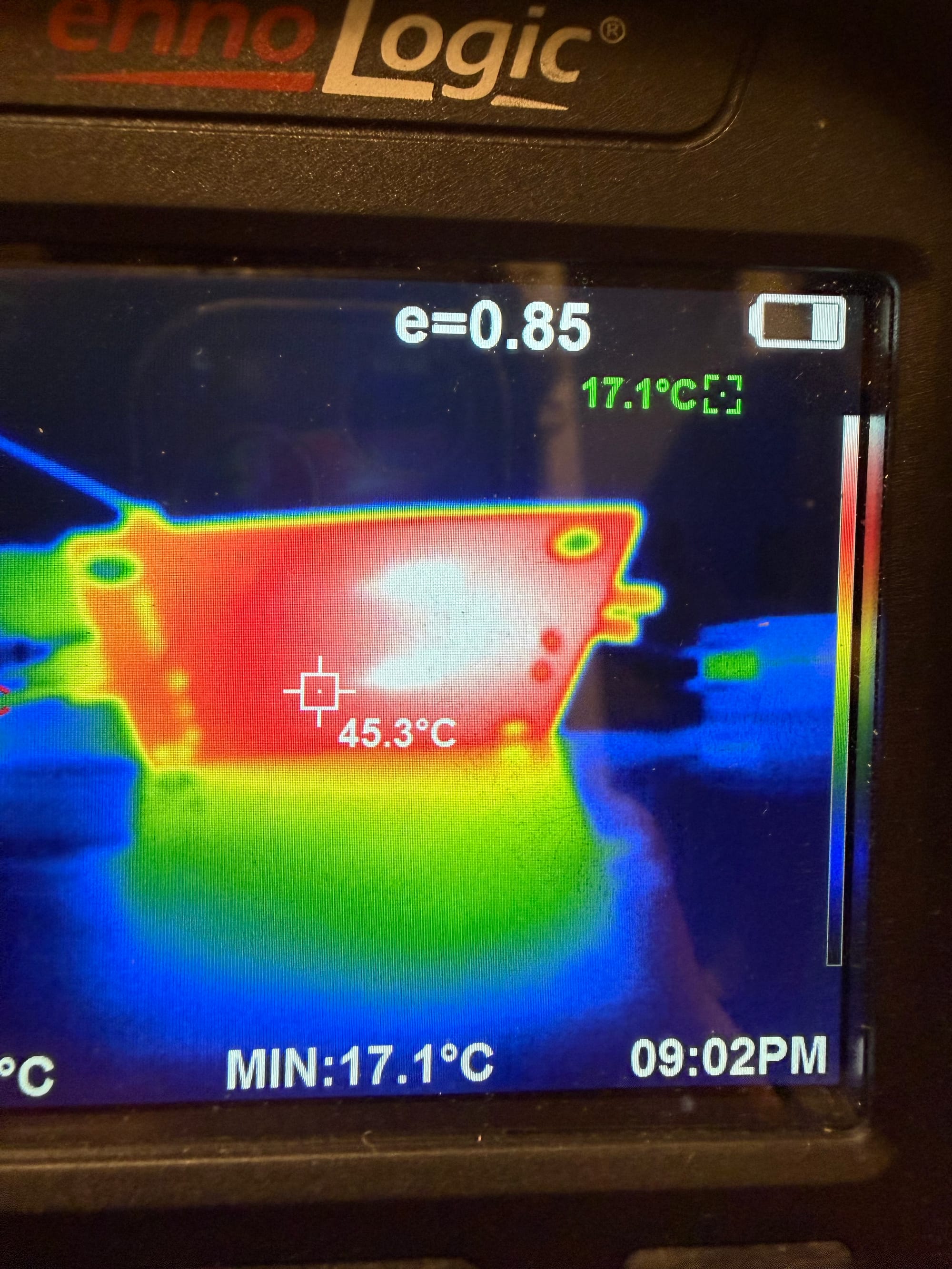
Actually...after testing it out with a practice transformer on 5/2/26 and using an infrared camera to check thermals, I believe some of the power traces are heating more than I want them to. While drawing 3A at 30VDC, the H-Bridge heated up in a few spots corresponding to power trace width bottlenecks. I somewhat predicted this when designing the PCB, but assumed the width would be good enough. I think for my general use this will "work", but in addition to the missing pull-down resistors on the gate inputs, I think I should redesign the PCB, and try to improve it for:
- Improved heat dissipation & current capacity by adding more thermal vias, widening power traces, and exposing the power traces to air to be tinned and passively air-cooled.
- Increased maximum voltage by implementing more clearance, creepage, SiC MOSFETs, and perhaps a better, isolated gate driver config.
- Increased maximum current by exposing the power traces to air to be tinned and not allowing bottlenecks of trace width.
- Adding pull-down resistors on the gate inputs.
- Adding reverse-polarity protection through a P-type MOSFET, zener diode, and gate resistor as explained in this reverse polarity protection app note: https://resources.pcb.cadence.com/blog/simple-solutions-for-reverse-polarity-protection
- Snubber suppression via RC or RCD passive snubbing since the plasma ignition transients can throw off ZVS operation and produce high-voltage spikes. Ideally, the transformer and LLC tank in general is designed to account for circuit parasitics, but because of time-dependent plasma capacitance changes as surface DBD plasma extends and retracts across the surface of the actuator, high-voltage transients may be reflected to the primary.
New:
Now I am updating this design with a new set of fixed parameters based on my lab's goals that have solidified further:
- 100V input, 200V output
- 5A input current (overkill, but allows for expansion in the future)
- 7kHz switching frequency with phase-shift modulation (doesn't modify the switching frequency)
So for these goals I am picking the following parameters for initial SPICE simulations, which I will then adjust as I notice problems:
- For the MOSFET, I require some margin above 100V, and I desire low ON resistance and gate charge. The Infineon SiC MOSFET IMT40R045M2H has a low 45mohm ON resistance, continuous current rating of 43A, gate charge of 21nC, and drain-source breakdown voltage of 400V which should be more than enough to satisfy the requirements and provide reasonably low switching and conduction loss.
- For the gate drivers, I think the UCC21550A will work best, because of the high 4A/6A source/sink drive current and safety circuitry it has within, like the disable pin, and controllable dead-time.
- To supply VCCI (5[V]) and VDDA/B (12[V]) on the gate drivers, I'm going to use a DC/DC converter module for 12[V] and an LDO for 5[V]. For the module, I need an input voltage range containing the 6S battery pack range of 18-25.2[V] to output 12[V]. On Digikey the part satisfying this requirement the best is the R-78K12-0.5 which outputs 6[W]. This should be more than enough continuous power for the gate drivers, since the peak current will be supplied by the capacitors. For VCCI, the supply current is just for the logic on the primary side, so I can use the quiescent current of 5[mA] max as an estimate to show that the current consumption is small and I can thus use a small voltage regulator to avoid complexity with having another SMPS voltage supply. Thus I'll use the AS78L05RTR-E1 with 100[mA] output current maximum at 5[V].
- For the signal input resistors and capacitors, I'll copy the datasheet example for now, \(33[pF]\) and \(51[\Omega]\).
- For the bypass capacitors, I'll use one at VCCI rated \(50[V]\) and \(200[nF]\) like the datasheet recommends. The bootstrap capacitor minimum is calculated by \(C_{boot}=\frac{Q_{total}}{\Delta V_{VDDA}}=\frac{351[nC]}{2[V]}=175.5[nF]\) and in the example, >5x margin was given, so I'll follow suit and choose \(C_{boot}=1.2[\mu F]\). Since I am choosing the A model, VDD minimum is 6.5[V] so I don't have to worry about encroaching on UVLO threshold due to droop.
- For the bootstrap diode in the UCC21550A, it recommends a Schottky diode with low forward voltage drop, >1.5x DC bus voltage, and \(I_{repetitive,max} \geq \frac{V_{DD}-V_{BDF}}{R_{boot}}\), where \(1<R_{boot}<20\). For this reason I'm picking the STPS2150 and \(2.2\Omega\) bootstrap resistor so the peak diode current is \((12-0.9)/2.2 \approx 5[A]\). The VDDB capacitor in the example consists of a 220[nF] and a 10[\mu F] capacitor which I will copy as well.
- From equations (3),(4),(7), and (8) in the UCC21550 datasheet, it calculates sink and source currents for estimated values of \(R_{ON}\) and \(R_{OFF}\) with bootstrap diode forward voltage of \(0.9[V]\), internal gate resistance of \(8.7[\Omega]\), \(R_{OH}=1.47[\Omega]||5[\Omega]\), \(R_{OL}=0.55[\Omega]\), and anti-parallel diode forward voltage drop (the datasheet example uses MSS1P3, so I'll use the same. The gate drive voltage is only 12V so a high blocking voltage diode isn't needed, and the example is 100kHz so the switching requirements are more than satisfactory for me) \(0.75[V]\). I'll start simulations with resistances around \(5-30[\Omega]\) and tune, so the gate drive current is high but not too high to cause ringing or excess power loss.
- I'll pick an initial \(R_{GS}=10[k\Omega]\) for simulations and tune, since the datasheet says 5-20 is typical.
- For dead-time,
Now here is the initial schematic I'll use for simulation:
The KiCad simulation process goes like this: